Description
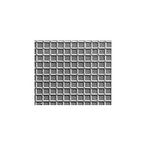
DESCRIPTION Useful for magnification calibration or image distortion check in SEM and LM. Single crystal silicon, 5mm x 5mm. The squares repeat every 10µm (0.01mm). The dividing lines are about 1.9µm wide, formed by electron beam lithography. A broader marking line is written every 500µm (0.5mm) which is useful for light microscopy. Lines are etched, and approximately 300nm deep. Available unmounted or mounted on SEM specimen mounts. A certificate of calibration can be supplied for the Silicon Test Specimen at extra cost. See information on mounts A-R Many types of samples can be mounted directly onto the Silicon Test Specimen so that an internal calibration is obtained in the image. Thickness: 675µm
Si crystal orientation:
Wafer type: P-type/boron doped
Resistance: 1-30 Ohm/cm To avoid contamination of test and calibration samples, we recommend storing these under vacuum. For the standard SEM pin mounts, the #16179 PELCO® SEM Sample Stub Vacuum Desiccator would be ideal. PELCO® Technical Notes, Planotec Test Specimen (148KB PDF) Planotec Silicon Test Specimens with calibration certificate for mounted test specimens only. The guaranteed accuracy is 1%. The basic reference specimen is calibrated by the National Physical Laboratory (counter part of NIST), of England, by laser beam interferometry. Sample Certification for Planotec Test Specimen (796KB PDF)